

The $3.8 Billion Global Track Market
Table 1. Global Photoresist Track Equipment Revenues and Market Shares
The Opportunity Beyond 300mm Silicon Manufacturing
Table 2. Global Photoresist Track Equipment Revenues by Wafer Diameter, 2025 ($ Millions)
Specialty Semiconductors and AI Infrastructure
Table 3. Global Photoresist Track Equipment Revenues by Application, 2025 ($ Millions)
Track Architecture and Manufacturing Economics
S-Cubed’s Quad Z Trac Challenges Conventional Architecture
The Manufacturing Economics of the Quad Z Architecture
Table 4. Conventional Track Architecture and S-Cubed Quad Z Trac
Specialty Applications and the 300mm Expansion Path
Investor Takeaway
Semiconductor investment has become increasingly concentrated on artificial intelligence, advanced logic, high-bandwidth memory and the capital equipment required to support next-generation computing. Much of the attention falls on lithography exposure, particularly EUV systems. Yet exposure is only one part of patterning. Photoresist coating and developing tracks are equally essential to applying resist, controlling thermal cycles and developing the patterns used in subsequent fabrication steps.
Track performance affects coating uniformity, thermal control, defectivity, throughput and ultimately manufacturing economics. This matters not only in high-volume 300mm silicon fabs, but also in compound semiconductors, photonics, MEMS, power devices and advanced packaging, where substrate materials, resist thicknesses, wafer sizes and production volumes can differ substantially from mainstream logic and memory manufacturing.
These specialty markets are becoming more important as AI infrastructure expands demand for optical communications, power management and heterogeneous packaging. That creates an opportunity for equipment architectures emphasizing wafer-handling efficiency, processing flexibility, compact footprint and cost of ownership. S-Cubed’s Quad Z Trac addresses those requirements with a distinctive multi-end-effector wafer-handling architecture designed initially for specialty manufacturing and intended to scale to 300mm.
The global photoresist track equipment market is dominated by Tokyo Electron (TEL), whose CLEAN TRACK family has a strong position in advanced semiconductor manufacturing. SCREEN Semiconductor Solutions, SEMES and China’s Kingsemi also participate, alongside smaller suppliers serving specialty applications. Data for this article and tables came from my report at The Information Network entitled “Global Semiconductor Equipment” Markets, Market Shares, Market Forecasts.”
The Information Network estimates global track equipment revenues at approximately $3.88 billion in 2024 and $3.78 billion in 2025. TEL accounted for an estimated 86.6% of the 2025 market. The data also show why overall market share can obscure competitive conditions in specialty manufacturing, where smaller wafers, unusual substrates and different production economics can create room for alternative equipment architectures.
According to Table 1, the global photoresist track equipment market declined modestly from an estimated $3.88 billion in 2024 to $3.78 billion in 2025, a decrease of 2.6%. Tokyo Electron maintained its dominant position with an estimated 86.6% market share in 2025, followed by SEMES at 4.4%, SCREEN at 4.0%, and Kingsemi at 3.4%. This concentration reflects the importance of established equipment platforms in high-volume semiconductor manufacturing. However, overall market share does not fully capture the opportunities available to smaller suppliers serving specialty semiconductor manufacturers, whose requirements for wafer handling, substrate flexibility, and equipment footprint differ from those of mainstream silicon fabs.
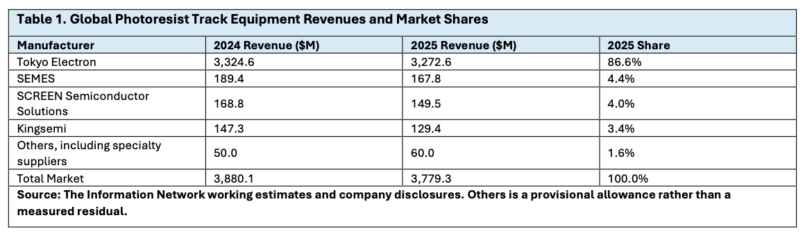
TEL’s leadership is concentrated largely in sophisticated systems supporting high-volume silicon manufacturing. Specialty fabs often place comparatively greater emphasis on substrate flexibility, equipment footprint, capital cost, small-lot efficiency and the ability to process multiple products on a common platform.
The market is heavily weighted toward 300mm manufacturing, but 200mm and smaller wafers remain important in compound semiconductors, MEMS, photonics, analog and power electronics. The Information Network’s model assigns approximately $3.33 billion, or 88.1%, of 2025 track revenues to 300mm systems and $449.3 million, or 11.9%, to 200mm and smaller systems.
According to Table 2, 300mm wafer processing accounted for approximately $3.33 billion, or 88.1%, of global photoresist track equipment revenues in 2025. The remaining $449.3 million was associated with 200mm and smaller wafers, representing 11.9% of the market. Although considerably smaller in revenue, this segment serves important applications in compound semiconductors, photonics, MEMS, and power electronics, where specialized substrates and manufacturing requirements create opportunities for alternative equipment architectures. For S-Cubed, this represents an immediate commercial opportunity, while the potential scalability of Quad Z to 300mm provides access to a substantially larger addressable market.
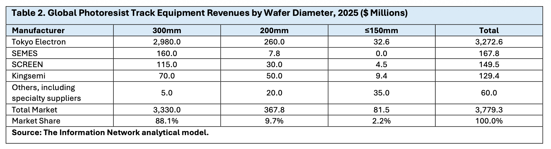
The smaller-wafer segment is particularly relevant to S-Cubed’s initial positioning. Many specialty fabs operate mature facilities where adding capacity without expanding cleanroom space can have substantial economic value. The much larger 300mm category represents a longer-term opportunity if the Quad Z architecture is qualified for production at that diameter.
AI infrastructure increasingly depends on technologies manufactured outside conventional leading-edge silicon. Photonics supports high-speed optical communications; GaAs and InP enable important RF and optoelectronic functions; GaN and SiC contribute to efficient power conversion; and advanced packaging uses additional lithography steps for redistribution layers, bumping and heterogeneous integration.
The Information Network estimates that silicon front-end manufacturing accounted for approximately $3.40 billion in 2025 track revenue, advanced packaging for $243.8 million, and specialty applications involving compound semiconductors, MEMS, photonics and power devices for $140.5 million.
According to Table 3, silicon front-end manufacturing accounted for approximately $3.40 billion, or 89.8%, of global photoresist track equipment revenues in 2025. Advanced packaging contributed $243.8 million, or 6.5%, while specialty applications, including compound semiconductors, MEMS, photonics, and power devices, represented $140.5 million, or 3.7%. Together, advanced packaging and specialty applications accounted for approximately $384.3 million in equipment revenues. These segments are particularly relevant to the expansion of AI infrastructure, which increasingly depends on optical interconnects, efficient power conversion, and heterogeneous semiconductor integration. Their manufacturing requirements create opportunities for suppliers capable of providing flexible processing and efficient wafer handling.
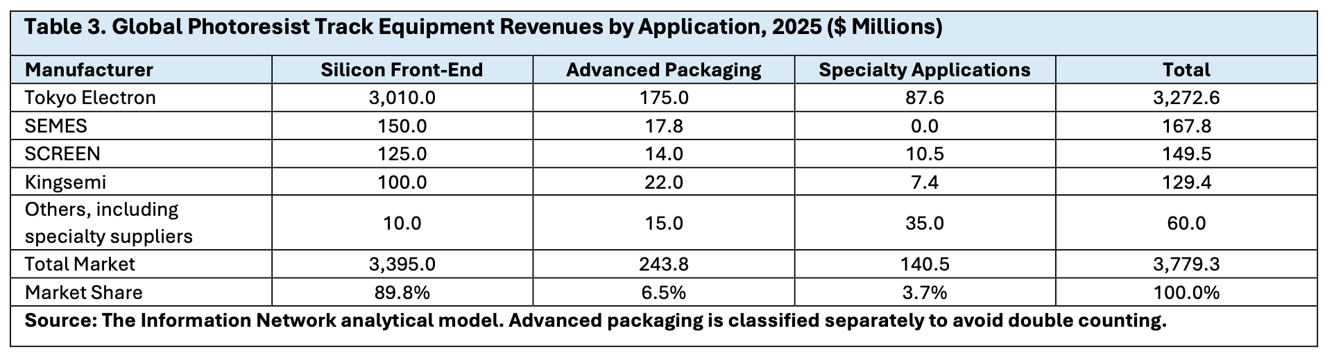
Wafer diameter and application are different classifications of the same market and should not be combined. The strategic point is that specialty manufacturers often value flexible processing, unusual-substrate capability, compact footprints and efficient handling of smaller production lots.
Track architecture can be a significant determinant of manufacturing economics. Conventional systems integrate coating, developing, thermal processing, chemical delivery and wafer handling into coordinated platforms. As module count increases, wafer transport can become a limiting resource if the handling system cannot supply and remove wafers quickly enough to keep process stations utilized.
Two architectural characteristics are particularly useful when evaluating wafer handling: the number of available end effectors and the number of controlled motion axes. More end effectors can increase the number of wafers immediately available for movement or exchange. Fewer required axes reduce the number of actuators, drives, sensors and motions inherent in the mechanism. Neither metric alone determines system performance, but together they provide useful indicators of transport capability and mechanical complexity.
Footprint matters as well. Cleanroom expansion can require substantial investment in environmental controls, chemical distribution, exhaust and supporting infrastructure. An architecture that increases useful processing capacity within existing space can therefore create value beyond nominal wafers-per-hour comparisons.
S-Cubed, a New Jersey semiconductor equipment manufacturer with decades of experience in photoresist processing, developed Quad Z Trac as an alternative to conventional central-robot architecture. The centerpiece is a three-axis process robot with four end effectors, supported by a five-axis front-end robot with two end effectors.
Rather than relying primarily on additional robot movements to service process modules, Quad Z stages multiple wafers for exchange. S-Cubed describes the result as a move-swap approach rather than a swap-move-swap sequence. By removing a completed wafer while having the replacement immediately available, the architecture is intended to reduce unproductive transfer movement and increase process-module utilization. The benefit is greatest when wafer transport constrains module utilization, making representative customer recipes the appropriate basis for comparison.
S-Cubed reports that Quad Z can accommodate roughly twice as many process modules within a footprint comparable to certain conventional central-robot configurations. The company specifies less than 25 square feet, including the chemical cabinet, for its compact 200mm implementation. Its FLEXI development platform and Quad Z also share related processing approaches, creating a potential path from development recipes to production equipment.
For specialty manufacturing, the most useful economic measure is cost per good wafer rather than headline throughput alone. Capital cost, utilization, floor space, maintenance, process flexibility, yield and qualification burden all contribute to the result.
Quad Z addresses these factors through four related design choices: four process-robot end effectors intended to reduce idle transfer movements; a three-axis process robot intended to limit mechanical complexity; modular architecture designed to provide high process-station density in a compact footprint; and support for varied substrates and processes. The potential advantage is cumulative: more effective scheduling can improve utilization while compact equipment and reduced mechanical complexity can lower facility and maintenance burdens.
Quantitative advantages in cost per good wafer will ultimately need to be demonstrated through application-specific customer data, including representative measurements of throughput, yield, defectivity, uptime and maintenance.
According to Table 4, S-Cubed’s Quad Z Trac differs from the conventional reference architecture principally in its wafer-handling configuration. Its process robot incorporates four end effectors and three controlled motion axes, compared with the representative conventional configuration of two end effectors and five axes. The additional end effectors provide greater wafer-staging capability, while the reduced number of motion axes can lower mechanical complexity, component requirements, and potential maintenance points. Combined with its move-swap wafer-exchange approach and compact modular design, these characteristics provide the engineering basis for Quad Z’s potential advantages in processing-module utilization, cleanroom footprint, and manufacturing economics.
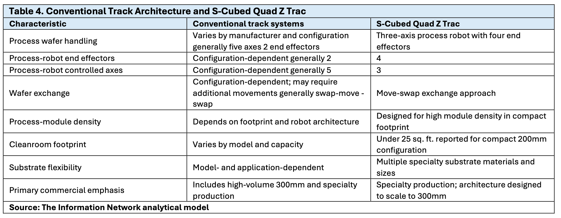
The comparison focuses on architectural characteristics rather than universal performance claims. Customers can evaluate these design choices against their own recipes, module requirements, throughput targets and ownership costs.
S-Cubed’s immediate opportunity is in applications where conventional high-volume silicon equipment may not align with customer requirements. Compound semiconductor, photonics, MEMS, power-device and advanced-packaging manufacturers often need flexible resist processing, support for nonstandard substrates and efficient handling of relatively small lots.
Quad Z is designed for multiple wafer materials and diameters, including silicon, GaAs, InP, germanium and lithium niobate. S-Cubed reports experience handling thousands of III-V compound-semiconductor wafers without breakage. Its modular approach also allows customers to add production capability without adopting a large fixed configuration at the outset.
The longer-term strategic opportunity is 300mm. S-Cubed describes the architecture as scalable to that wafer diameter, which would place it against a much larger market. Success there would require qualification to the stringent process uniformity, contamination, throughput and uptime expectations of advanced silicon manufacturing. The architectural concept may scale; production competitiveness must be established in the target application.
The approximately $3.78 billion global photoresist track market is highly concentrated, but its economics vary materially by wafer size and end use. The estimated $449 million market for 200mm and smaller-wafer equipment includes applications where substrate flexibility, compact footprint, small-lot efficiency and capital utilization can matter as much as maximum nominal throughput. Photonics, compound semiconductors, power electronics and advanced packaging also connect these specialty requirements increasingly to AI infrastructure.
S-Cubed’s Quad Z Trac offers a distinct architectural proposition: a three-axis, four-end-effector process robot; move-swap wafer exchange; modular processing; and a compact reported footprint. The differentiation is not simply a smaller track, but a different approach to wafer handling intended to improve module utilization while reducing unnecessary motion and mechanical complexity.
The longer-term opportunity extends to 300mm, a market several times larger than the smaller-wafer segment. Qualification and customer data will determine the magnitude of the economic advantage, but the architecture merits attention because semiconductor equipment innovation includes not only process chemistry and transistor scaling, but also the mechanics by which wafers are moved, processed and converted into productive fab capacity.